

Anderon, an IBM company, said Wednesday that it has finalized a $1 billion award from the U.S. Department of Commerce under the CHIPS and Science Act, paired with a separate $1 billion IBM commitment, to accelerate quantum-wafer R&D in Albany, New York. The announcement matters because it moves a much-discussed idea in quantum hardware—a specialized domestic foundry model—from proposed incentive to funded operation, with IBM saying the first quantum wafers are already running through its 300-millimeter facility.
That still leaves the real business question unanswered: does this create a scalable manufacturing layer that other quantum builders can use, or does it mainly underwrite IBM’s own path to future systems? The most honest answer today is somewhere in between. The capital is real, the manufacturing site is real, and the 300mm process flow is more concrete than a lab-only effort. But the public evidence still says far more about IBM’s strategic buildout than it does about yield, repeatability, pricing, or customer access for the wider market.
From proposed incentive to funded manufacturing program
The important change this week is not that Anderon exists. IBM and the Commerce Department had already disclosed that plan in May, when they announced a letter of intent for what IBM described as America’s first purpose-built pure-play quantum foundry and a proposed $1 billion CHIPS award. The September update turns that proposal into a finalized award.
That shift matters for anyone trying to judge whether quantum manufacturing is becoming an investable supply-chain layer rather than a collection of bespoke physics projects. A signed award is more concrete than an intent letter. It makes planning easier for suppliers, researchers, prospective customers, and policymakers watching whether CHIPS money is reaching technologies beyond classical semiconductors.
It also sharpens the economics. IBM has said its own contribution totals $1 billion, alongside intellectual property, assets, fabrication expertise, and specialized talent. What the public materials do not provide is the breakdown between cash and in-kind support, the timing of that spending, or the award’s milestone structure and payment schedule. Those omissions are not minor. In manufacturing, the difference between a headline commitment and a disbursed, milestone-tied program often determines how quickly process development turns into dependable output.
The same is true for Anderon itself. IBM introduced it in May as a standalone company headquartered in Albany, with Mukesh Khare as CEO, but the available materials do not spell out the governance, customer-access rules, or legal separation that outside users would want to understand before trusting a foundry that is also tied to a major hardware developer.
Why 300mm matters—and why it is not the proof point
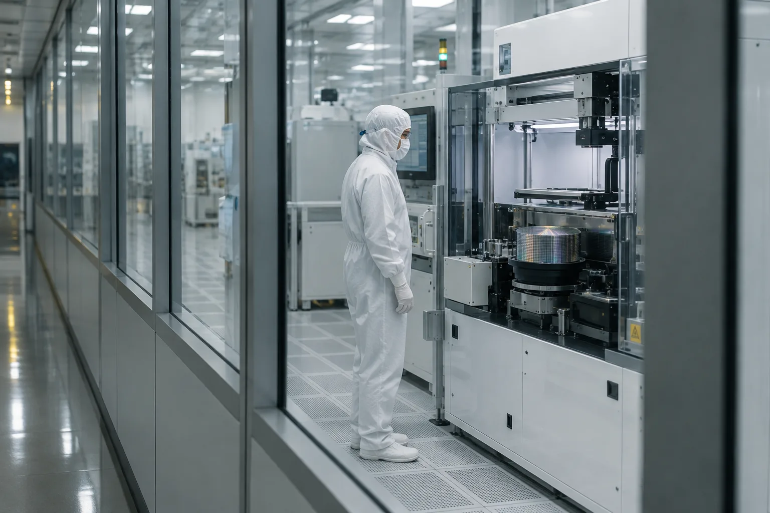
The clearest operational rationale behind Anderon is its use of 300mm wafers, the standard 12-inch format common in advanced semiconductor manufacturing. IBM has already described 300mm quantum fabrication as part of its own workflow for its Loon and Nighthawk chips at the NY CREATES Albany NanoTech Complex. The attraction is straightforward: larger wafers and automated 300mm tools can, in principle, produce more chips per run and do it in a more standardized environment than smaller, more customized lines.
That is the strongest practical reason to take this announcement seriously. Quantum hardware does not scale just by inventing better qubits in a lab. It has to survive process variation, material defects, wiring complexity, packaging challenges, cryogenic integration, and repeated fabrication cycles. A 24/7 semiconductor R&D environment such as Albany’s can provide tighter process control, better metrology, and faster iteration than a fragmented one-off approach.
But wafer diameter is not the same as manufacturing readiness. Quantum devices are unusually sensitive to microscopic defects, material interfaces, electromagnetic noise, and assembly choices that might be tolerable in conventional chips. IBM’s own technical description of the flow makes that clear. The Albany step is only part of the chain; wafers may then receive custom processing at Yorktown, followed by 3D stacking, control-electronics connections, and testing in dilution refrigerators.
That broader flow is what makes Anderon potentially useful. Its wafer stack can include superconducting wiring, through-silicon vias, and bump bonds, all of which matter for denser qubit arrays and signal routing. Just as important, IBM says 200mm lines still have a role for custom or especially difficult research steps, which is a reminder that the industry is not simply “graduating” from small wafers to big ones. It is trying to combine the flexibility of quantum R&D with the discipline of semiconductor process control.
The missing proof points are the ones customers and investors actually need: usable die per wafer, defect density, cycle time, repeatability across lots, coherence, error rates, and cost. The first wafers running through a facility is an important milestone. It is not the same thing as qualified, high-yield production.
What would make this a true foundry rather than an IBM-funded pipeline
The case for public support is easy to understand. Quantum hardware is capital intensive, talent constrained, and still too early for many startups or research institutions to justify building their own full fabrication stack. A specialized foundry could lower those barriers and keep more process know-how in the United States. That is the industrial-policy logic behind pairing CHIPS funding with a large corporate anchor.
The question is whether the resulting platform becomes broadly usable. Anderon’s initial focus is on high-performance superconducting qubit arrays, quantum input/output signaling, and readout signal-chain components, with other modalities planned over time. That is a meaningful starting point, but it also means the foundry is not yet a universal quantum manufacturing utility.
For outside companies, the next set of facts matters more than the size of the award. Can customers access process-design kits and design rules? Can they reserve capacity without exposing sensitive IP to a foundry tied to IBM’s own roadmap? Are there qualification lots, process windows, packaging handoffs, and quality controls that let an external team move from prototype to repeatable supply? Will Anderon publish wafer-level or system-level data showing that more automated fabrication improves actual device performance rather than just throughput?
Those questions matter well beyond startups. National labs and defense programs want reliable domestic sources for specialized hardware. Universities want fabrication access without having to recreate a full semiconductor workflow. Enterprise technology leaders and investors want to know whether this shortens the path from headline qubit counts to usable systems. And IBM itself needs the foundry to serve its internal roadmap, including its long-term fault-tolerant ambitions.
That creates a tension at the center of the story. IBM may be the customer best positioned to keep the line busy, accelerate learning curves, and justify the investment. At the same time, if the public outcome is mostly a captive manufacturing channel for IBM, the broader foundry thesis will remain unproven.
For now, Anderon looks less like a finished quantum manufacturing platform than a serious, well-funded manufacturing experiment with a real anchor customer and a strategically important location. If IBM and Anderon begin showing qualification results, repeatability data, and credible external customer access, the $2 billion backing will look like the foundation of a new supply-chain layer. If those signals do not appear, the announcement will read more as subsidized vertical integration than as the opening of a shared quantum foundry market.

 By
By
 By
By


 By
By
 By
By
 By
By