



On Sept. 16, Reuters reported that SK hynix was discussing ways to make memory chips in the United States with Intel. Hours later, in a same-day newsroom clarification, SK hynix said no plan, agreement, or decision had been finalized. That matters because the denial does not make the story trivial; it makes it legible. The market is getting a glimpse of how seriously AI-memory localization is being explored, even though nothing public yet shows a signed transaction.
The practical question for customers, suppliers, and investors is straightforward: is this the start of an actual U.S. memory-fabrication deal, or mainly a signal that AI demand, U.S. industrial policy, and Intel’s unfinished Ohio capacity are converging before the economics are settled? For now, the second reading fits the record better. The reported scenarios are consequential, but the only committed SK hynix manufacturing project in the U.S. is a packaging and R&D site in Indiana, not a front-end memory fab in Ohio.
What is actually being discussed
SK hynix’s clarification is unusually useful because it names the two scenarios described in the report rather than waving them away. One is leasing part of Intel’s planned Ohio One semiconductor campus. The other is a joint venture involving SK hynix, Intel, and large cloud companies. Then comes the key sentence: neither has been decided.
That distinction is more than legal housekeeping. If SK hynix were merely dismissing a baseless rumor, it would not need to identify potential structures so specifically. But the same statement also blocks the market from treating those structures as a transaction. There is no public term sheet, no chosen facility module, no product definition, no capital budget, no ownership split, no customer commitment, and no start date.
Those missing details are not minor. “Memory-chip production” could mean commodity DRAM, HBM-related front-end wafer processing, another memory category, or only packaging and test. Each path uses different equipment, engineering talent, qualification flows, and cost assumptions. Until the product and process are identified, the headline is strategically suggestive but operationally incomplete.
Indiana is committed; Ohio is still a timeline
The clearest way to read this story is to separate confirmed U.S. capacity from exploratory options. In August, SK hynix’s Indiana groundbreaking announcement laid out a specific plan for an advanced-packaging and R&D facility in West Lafayette focused on next-generation HBM. The company said it expects to invest more than $4 billion, open the cleanroom by October 2028, and begin mass production in the second half of 2029.
That project is substantial, but it is also narrowly defined. SK hynix’s model for Indiana is Korea-to-Indiana: wafers are to be produced in Korea, then packaged and tested in Indiana before delivery in the U.S. The company has said the site is expected to employ about 1,000 people commercially, is considering more than 100 suppliers, and could support roughly 7,000 direct and indirect jobs across construction and operations.
Ohio is a different proposition. In Intel’s February 2025 construction update, the company described more than $28 billion of planned investment in two leading-edge fabs at New Albany. But it also set a long runway: Mod 1 construction was planned for completion in 2030, with operations between 2030 and 2031, while Mod 2 was planned for completion in 2031 with operations in 2032. Intel’s update did not mention SK hynix or a memory-production partnership.
That gap in maturity is the point. Indiana is a defined back-end HBM node with dates, staffing, and a production model. Ohio is a future front-end manufacturing campus whose productive use remains years away. Leasing space there could save time on site development compared with building from scratch, but it would not by itself solve the harder parts of semiconductor manufacturing: tool installation, memory-process integration, utility readiness, cleanroom qualification, yield ramp, workforce training, customer approval, and the intellectual-property and export-control questions that can shape cross-company manufacturing arrangements.
Why AI memory makes this more than a rumor story
AI infrastructure has made memory less interchangeable than the old commodity framing suggests. High-bandwidth memory sits next to accelerators in many AI systems, and supply is constrained not just by wafers but by packaging capacity, power, and qualification with major customers. That is why a U.S. footprint has appeal even before it pencils out perfectly on paper. It can improve resilience, bring supply closer to hyperscaler demand, reduce exposure to trade friction, and answer political pressure to localize more of the semiconductor stack.
That does not mean any U.S. memory plan is automatically valuable. Packaging and fabrication are not interchangeable. SK hynix’s Indiana site addresses one important bottleneck in the HBM chain, but it still depends on Korean wafer output. A separate Ohio arrangement, if one ever emerges, would answer a different question: whether part of that front-end memory production can also move closer to U.S. customers.
The reported joint-venture option points to another mechanism worth watching. If cloud companies participate, the logic changes from a standard supplier expansion to a supply-assurance play. Hyperscalers could seek influence over capacity allocation or future output, while SK hynix and Intel would have to work through capital contributions, product ownership, operating control, and risk sharing. None of those terms is public, and without them the strategic outline is clearer than the business case.
What would count as proof
If this story advances from exploration to commitment, the market will need more than a headline about making memory in America. A credible announcement would have to specify what product is involved, whether the project adds wafer starts or only expands packaging and test, which Ohio module or site is being used, how much capital each party is putting in, whether a cloud customer is committing volume, and when tool installation and cleanroom readiness translate into qualified output.
Just as important, any real deal would need to explain how it connects to Indiana. Does Ohio feed wafers into SK hynix’s HBM packaging plan in West Lafayette, or is it aimed at a different memory line altogether? Who bears construction risk and yield risk? How would public incentives be treated? When would customers be able to buy dependable, economically priced product rather than symbolic domestic capacity?
Until those answers appear, the official clarification sets the right frame. SK hynix has not confirmed a U.S. memory-production deal with Intel. What it has confirmed, indirectly but meaningfully, is that the search for AI-memory localization options is real enough to warrant a public response. For device makers, cloud operators, and equipment suppliers, that is worth watching closely. It is not yet proof that U.S.-made memory is coming soon; it is proof that the pressure to build it is getting harder to ignore.

 By
By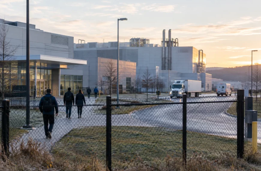
 By
By
 By
By
 By
By

 By
By