
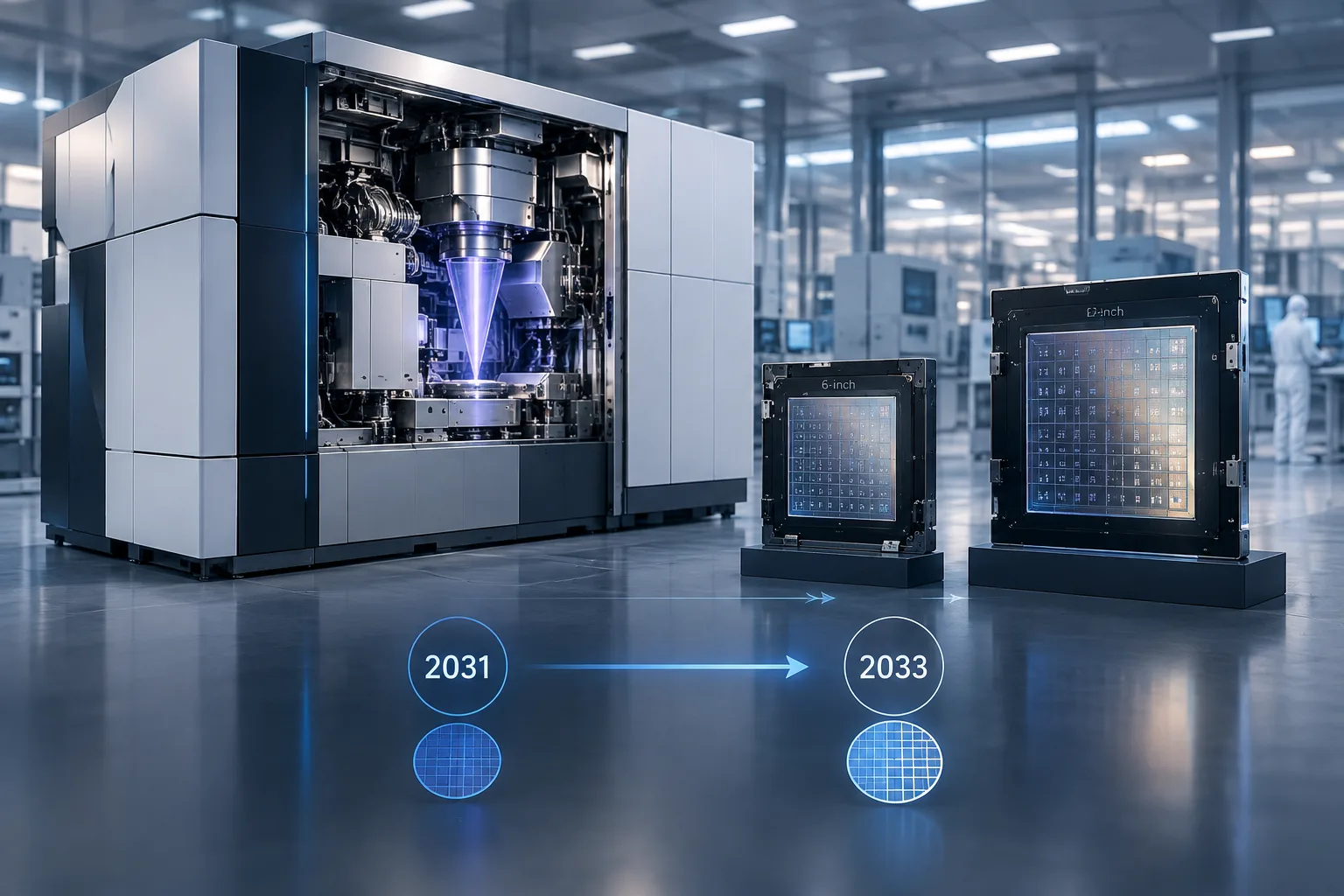

ASML and TSMC have put a concrete timetable on one of High-NA EUV’s least glamorous but most consequential problems: the mask format. In a joint statement from TSMC and ASML, the companies said they are launching an industry initiative to move High-NA EUV from the current 6-inch photomasks to 12-inch masks, with a pilot line targeted by 2031 and full lithography-system readiness for advanced-node production by 2033. That matters because High-NA can reach production sooner with today’s masks, but not at the most attractive long-run economics.
The real question for chip buyers and semiconductor planners is straightforward: can the industry remove a mask-format bottleneck before it turns High-NA into a tool that works technically but scales expensively? The answer, for now, is yes in principle, but only if the investment starts well before 2031 and spreads far beyond scanner purchases.
The bottleneck is moving from optics to infrastructure
High-NA EUV is not waiting for 12-inch masks to become useful. TSMC says it intends to use ASML’s High-NA technology in high-volume manufacturing for advanced nodes starting in 2030. And Intel and ASML said this month that customers can use High-NA with today’s 6-inch masks either by staying within the available field or by using stitching and process-design-kit support.
But that is a bridge, not the end state. ASML’s own EXE:5000 documentation makes clear why: High-NA’s anamorphic optics cut the exposure field to half the size used by current 0.33-NA EUV systems. That helps print finer features, but it also makes mask-area efficiency more precious. A format that is workable for early insertions can become restrictive when more layers, larger dies, and tighter design rules move onto the platform.
That is why the TSMC-ASML announcement is more important than a typical ecosystem press release. It effectively separates High-NA adoption into two economic phases. Phase one is 6-inch-mask High-NA, where the industry proves device performance, learns process windows, and absorbs the pain through floorplanning and selective stitching. Phase two is 12-inch-mask High-NA, where the ecosystem tries to recover scanner productivity, reduce mask-related non-recurring engineering, and remove stitching constraints before High-NA use broadens across more critical layers.
Where the spending shows up first
The headline names are ASML and TSMC, but the first visible capex will land across the mask supply chain.
Start with mask blanks. HOYA, which says it holds an exceptionally high share of the EUV mask-blank market, has already tied future capacity expansion to High-NA and planned a new Singapore plant with an initial investment of about ¥42 billion and start-up targeted for fiscal 2028. That is the kind of lead time this transition implies: years before the 2031 pilot line, suppliers need glass, multilayer, cleaning, and defect-control capacity lined up.
Then come the mask houses. TSMC’s statement says major ecosystem partners and suppliers have expressed interest, but the practical burden will fall on companies that write, etch, inspect, repair, clean, and qualify masks at much larger physical format and tighter tolerances. Tekscend Photomask’s footprint across Japan, Taiwan, the US, Germany, France, Singapore, Korea, and China shows why this is not one country’s project, even when customers want more regional resilience.
Inspection is another obvious spending pocket. Lasertec says its EUV mask-blank inspection tools are the de facto standard and that it has a large share in leading-edge mask inspection. That makes inspection capacity a likely choke point, not a background detail. If large-format masks raise the value of each reticle set, mask defectivity and review throughput matter more, not less.
The software stack also needs money earlier than many procurement teams assume. Intel’s public emphasis on stitching-aware PDK support today, and ASML’s broader push in computational lithography, are reminders that mask-format transitions are partly EDA transitions. Designers, OPC flows, and reticle data handling all have to adapt before the first pilot line is useful.
What it means for node cost and yield
High-NA’s appeal is familiar: higher resolution, fewer multi-patterning steps, and the possibility of better scaling economics. ASML says the EXE:5000 can print features 1.7 times smaller than current NXE EUV systems, achieve transistor densities 2.9 times higher, and improve imaging contrast. Those are powerful levers.
But they do not automatically lower cost at first insertion. Early High-NA layers still carry expensive masks, limited field flexibility, and fresh process-integration work. If fabs rely on stitching or design workarounds to stay on 6-inch masks, part of the scanner benefit gets paid back in mask complexity, design constraints, and verification overhead.
The 12-inch transition matters because it changes the amortization math. Larger masks should let fabs use High-NA on a broader set of layers without leaning as heavily on stitching. That can improve effective scanner productivity, spread mask NRE across more useful area, and reduce the yield risk that comes with additional overlay-sensitive handoffs. In other words, the announcement is not mainly about making the first High-NA products possible. It is about keeping later-node costs from bending upward too sharply as High-NA layer counts rise.
There is still uncertainty around where the savings show up first. They may arrive as fewer masks per design, better throughput on select bottleneck layers, or improved yield from simpler patterning. Different device makers will value those levers differently. Logic foundries chasing very large AI dies will care more about field constraints than companies using High-NA on a narrower subset of layers.
U.S. onshoring gains fabs, but not full independence
For US policy and procurement teams, the announcement is also a reminder that “onshoring” is not the same as localizing the full toolchain. TSMC Arizona now encompasses multiple planned logic fabs, advanced packaging facilities, and an R&D center, including a third fab slated for N2 and A16-class technologies by the end of the decade. That increases the odds that more advanced wafer processing and some downstream integration happen in the US.
But the core High-NA mask chain remains stubbornly multinational. ASML is in the Netherlands. ZEISS supplies the lithography optics from Germany. HOYA’s next mask-blank expansion is in Singapore. Key mask-shop capability remains distributed across Taiwan, Japan, Europe, and the US. Lasertec’s center of gravity is in Japan even as it supports customers globally. The TSMC-ASML plan may broaden participation, but nothing in the announcement suggests a fully domestic US 12-inch High-NA mask ecosystem is close.
That has two consequences. First, the most fragile lead times may sit in materials, inspection, and mask qualification rather than in the fab shell itself. Second, even buyers who welcome more US wafer capacity should expect cross-border dependencies to remain embedded in the most advanced node roadmap.
For the industry, the practical message is clear enough. High-NA is no longer just a scanner roadmap. It is now a mask-format conversion program with a date attached, and the companies that prepare earliest will not just secure supply. They will shape the cost curve of the next decade’s leading-edge chips.
 By
By

 By
By

 By
By
 By
By
 By
By