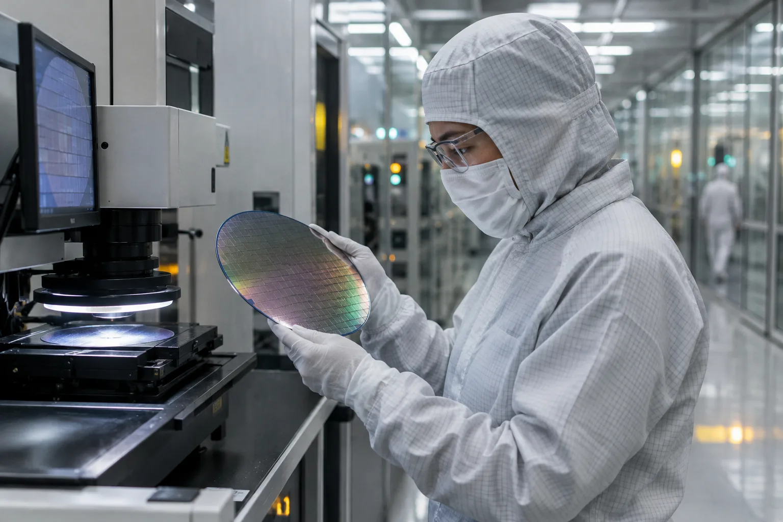


On October 5, Rapidus unveiled Rapidus CORE, a new ecosystem framework whose first phase is a 17-company Design Solution Associates group meant to help customers design chips for the company’s advanced 2nm process and carry those projects toward manufacturing. For Japan’s state-backed foundry gamble, that matters because a leading-edge fab is not commercially real just because a clean room exists or a process node has a name. Customers need a way in.
That makes the central question straightforward: does CORE turn Rapidus into a usable foundry platform, or is it still mainly a partner roster ahead of the harder proof points—actual tape-outs, wafer orders, stable yields, competitive pricing, and repeatable volume production?
Foundries are sold before silicon ships
Rapidus is trying to build something that only a few companies in the world currently do at the leading edge. As Reuters reported on October 7, the company has about $15 billion in Japanese state backing and needs to win customers ahead of planned 2-nanometer contract production in the second half of the next fiscal year. Reuters identified TSMC, Samsung Electronics, and Intel as the small group of leading-edge competitors that already combine manufacturing experience with mature customer ecosystems.
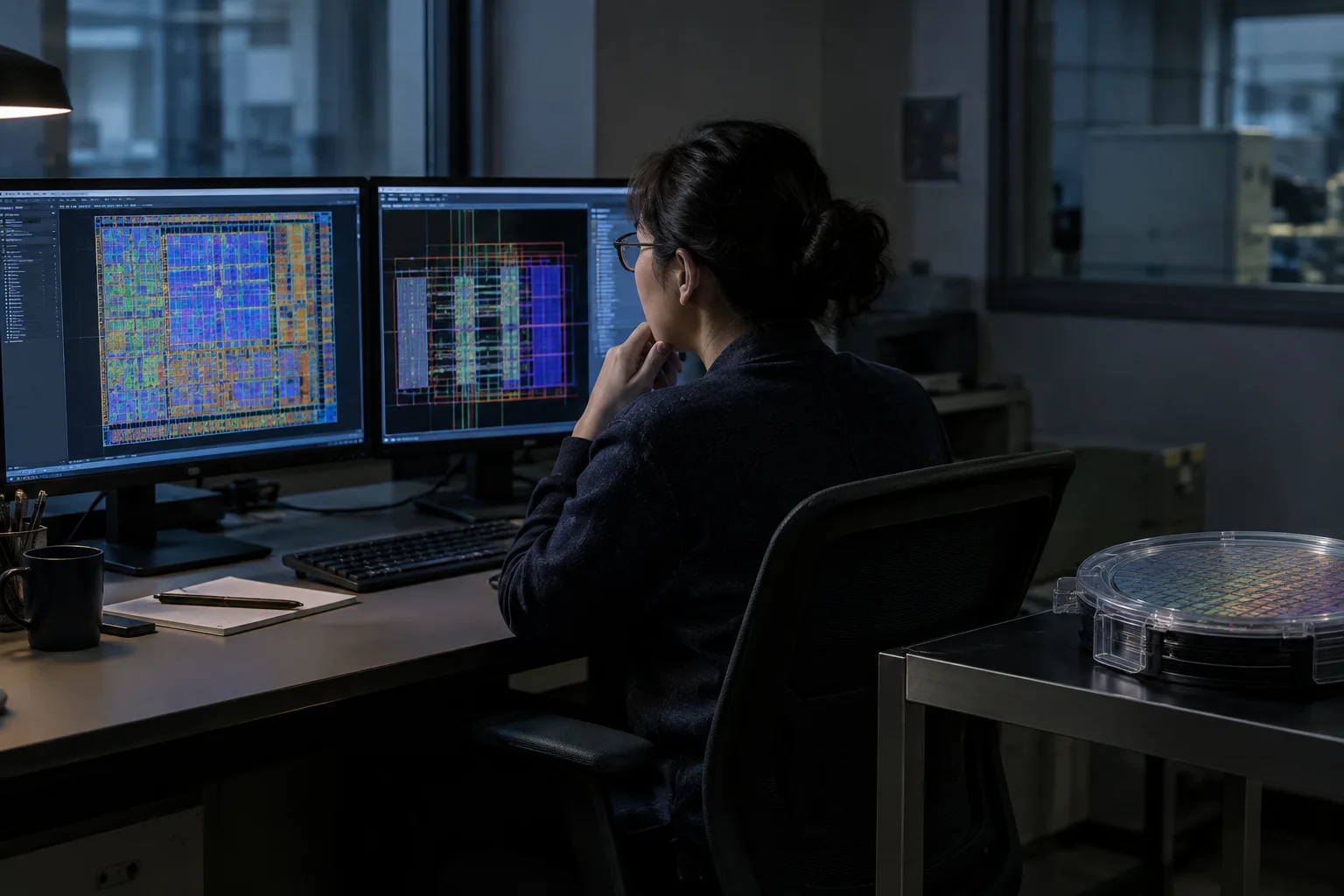
That last point is the reason CORE matters. A chip company cannot simply hand over a concept and wait for wafers. It needs a process-design kit, design rules, verified electronic-design automation flows, reusable intellectual property, physical implementation help, packaging and test options, and enough engineering capacity to get from idea to tape-out without discovering too late that key pieces are missing. Mature foundries sell that confidence long before they ship production silicon.
Rapidus is explicitly trying to assemble that confidence layer. In its October 5 announcement, the company said CORE is meant to integrate research institutions, EDA, IP, design, and manufacturing so customers in Japan and overseas can move from development to production on a single infrastructure. That is a practical answer to one of the biggest barriers facing any new foundry: even interested customers hesitate if onboarding looks expensive, slow, or risky.
The strategic backdrop is larger than one fab. Reuters noted that Japan’s share of the global semiconductor market has fallen from roughly 50% in the 1980s to less than 10% today. If Rapidus works, Japan gets more than a factory in Hokkaido. It gets a domestic anchor for materials, equipment, design, and manufacturing at a time when AI demand is increasing the value of leading-edge logic and governments want less dependence on a tightly concentrated supply chain.
What the 17 associates change
The immediate value of CORE is not that it proves customer demand. It is that it lowers the cost of exploring Rapidus.
The 17 named associates include Cadence Design Systems and Synopsys, engineering and IT services firms such as HCL Technologies, Infosys, Quest Global Services, and Wipro, and Japan-based printing and mask-related names including Dai Nippon Printing and TOPPAN, along with chip-design specialists such as AION Silicon, GreatAsic Technology, Oppstar Technology, and SkyeChip. Rapidus says these companies will help bridge customers to design resources and specialized expertise tied to its 2nm process.
In practice, that can matter a lot, especially for prospective customers that are not large enough to command top priority everywhere else. A new foundry needs more than flagship customers; it also needs a broad funnel of companies willing to try shuttle runs, prototypes, and first products. If CORE gives those customers a clearer path to physical design support, workflow setup, mask-related services, and manufacturing handoff, Rapidus becomes easier to evaluate.
The timing matters too. Data Center Dynamics reported that Rapidus began testing its first production line in Hokkaido in 2025 and is expected to start manufacturing 2nm chips in 2027. That makes 2026 and 2027 the period when customer enablement has to start hardening into real project pipelines.
What the announcement does not prove
The commercial gap is still large. Rapidus has not publicly identified signed foundry customers, committed wafer volumes, completed tape-outs, production yields, capacity reservations, pricing, or the commercial terms that govern participation by the 17 associates. The company has also not publicly shown which partner would provide which service on a given customer program, or whether each associate has committed dedicated resources rather than joining a framework.
That is why Reuters treated the move as incremental progress rather than evidence that the fab is already spoken for. A design network can reduce friction at the front end, but it does not guarantee that customers will risk a production program on a new process from a company founded in 2022. Reuters also pointed to a harder industry truth: running a leading-edge fab continuously, with stable yields and viable economics, is difficult even for established players. Samsung’s own struggles are a reminder that process leadership, yield learning, and commercial execution are separate hurdles.
There is also a switching-risk problem for customers. A company designing around TSMC today may want a second source or a geopolitical hedge, but moving a high-value chip to a new foundry is not like changing a cloud vendor. If first silicon misses, if yields lag, or if capacity is uncertain, there may be no fast path back into a mature leading-edge queue. That makes diversification attractive in theory and expensive in practice.
The scorecard that matters now
For designers and investors, the next useful question is not whether CORE sounds credible. It is which milestones would show that the ecosystem is becoming operational.
The leading indicators are the quality and revision pace of the PDK; availability of sign-off-capable EDA flows; access to silicon-proven IP; announced shuttle or prototype wafer schedules; and evidence that packaging and test options are lined up. The proof points come later and are harder to fake: a growing tape-out count, first-silicon results, improving defect density and yields, committed capacity, acceptable cycle times, workable wafer pricing, and a customer mix that is broader than a handful of subsidized experiments.
That is the standard Rapidus will ultimately be judged against. CORE is a sensible and probably necessary move because foundries are won in design enablement before they are won in production. But it is still pre-proof. The 17 associates make Rapidus easier to approach; they do not yet make the Hokkaido fab a trusted default for advanced chips. Until those markers start to appear, CORE looks best understood as serious customer-enablement infrastructure for a difficult industrial ramp—important, but not yet decisive.

 By
By
 By
By
 By
By
 By
By
 By
By

 By
By