

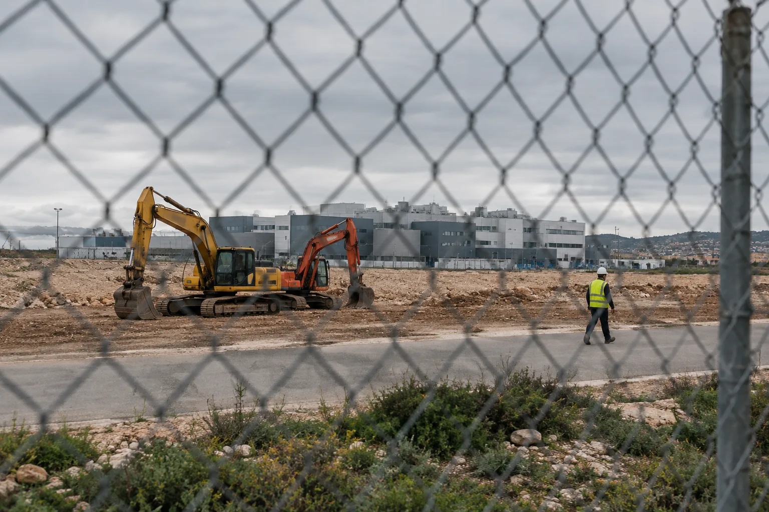

GlobalFoundries has started construction on a new 300mm semiconductor fab at its Malta, N.Y., campus, the first plant under a U.S.-Japan initiative announced in October that can provide up to $21 billion for two fabs at the site. The first facility is tied to an initial investment of about $10 billion, including $570 million in New York State incentives, and GF expects it to come online in 2029. That makes this more than a local groundbreaking: it is a live test of whether industrial policy and cross-border financing can turn into dependable U.S. chip supply for automakers, factory equipment makers and communications vendors.
The reader’s real question is not whether another fab building is going up. It is whether this model creates durable semiconductor resilience or mostly relocates one more stage of production while the harder constraints—customers, utilities, materials, packaging, workforce and ramp execution—stay unresolved. The answer, for now, is that the project could be important precisely because it targets foundational chips, but its value will be proved only if the site moves from construction to qualified, regularly utilized output.
A different way to add capacity
What distinguishes the Malta expansion is not just its size but its structure. In its announcement, GF said Japan will provide the investment while GF supplies the process technology, manufacturing expertise and operating capability. GF’s Nov. 4 SEC-filed third-quarter materials add an important detail: the company expects to be paid management and technology fees over the life of the project.
That matters because semiconductor fabs are capital-hungry, and this one is enormous relative to GF’s current operating scale. GF reported third-quarter 2026 revenue of $1.899 billion, a 30.1% gross margin and $647 million of adjusted EBITDA. A model in which outside capital funds the facility while GF operates it can expand U.S. manufacturing without forcing the foundry to absorb the full financial burden on its own balance sheet.
But the same structure creates a second question for investors and customers: how strong are the incentives once capital and operations are split? The public materials do not say how much of the roughly $10 billion comes directly from Japanese capital versus other financing, how fee income will vary with utilization, or how GF’s upside compares with owning the fab outright. Lower direct capital exposure can make expansion easier; it does not by itself guarantee that the fab will open on time, run at target yields or fill its capacity profitably.
Why mature-node supply is still strategic
The Malta project is aimed at a part of the market that receives less attention than AI accelerators but often causes more widespread disruption when it goes short. GF says the new capacity is intended for foundational semiconductors used in automotive, industrial, communications and connected-infrastructure applications. Those are the kinds of components that can idle an assembly line, delay grid equipment or hold up telecom hardware even when leading-edge chips remain available elsewhere.
GF estimates the first fab will add about 900,000 300mm wafers of annual U.S. manufacturing capacity when fully operational; a second planned fab is expected to add roughly the same amount as the broader initiative advances. If that capacity arrives on schedule and is qualified for real customer programs, it would meaningfully deepen domestic supply in a set of markets where sourcing assurance often matters more than bragging rights about the smallest process node.
The project also fits a broader buildout around Malta rather than a single isolated investment. GF already runs a major U.S. manufacturing base there. In October, the company said it would reallocate $955 million of existing U.S. CHIPS and Science Act incentives toward advanced manufacturing in Malta and Burlington, Vt., including silicon photonics and advanced packaging. Separately, GF has a multi-year $2 billion manufacturing agreement with TSMC for U.S.-based silicon interposers, with volume production expected to ramp in the first half of 2028. Together, those pieces suggest policymakers and customers are trying to turn the region into a more complete semiconductor node.
More complete is not the same as complete. A New York fab still depends on globally sourced equipment, chemicals, wafers, packaging, testing, logistics and utilities. Domestic wafer starts reduce some risks, especially for selected U.S. customers and public procurement, but they do not eliminate international chokepoints. That is why “made in New York” should be read as improved resilience, not supply-chain independence.
The milestones that matter more than the ceremony
For businesses deciding how much confidence to place in this project, the scoreboard starts now. The most important markers are not the job totals or the headline investment, but the operational milestones between groundbreaking and steady production: construction progress, tool installation, utility readiness, workforce recruitment and training, first wafer, customer qualification, yield ramp and sustained utilization.
Several of those items are still opaque. Public materials do not disclose the fab’s exact process nodes, product mix, wafer pricing, utility requirements, expected utilization or return profile. They also do not say which customers have reserved capacity, whether long-term offtake agreements are in place, or how output will be split among automotive, industrial, defense, communications and data-center-related demand. Without those commitments, capacity remains a possibility rather than dependable supply.
The workforce claims deserve the same practical reading. GF says the two-fab initiative could create about 27,000 construction and ecosystem jobs and more than 1,000 high-skilled manufacturing jobs in New York’s Capital Region. Those are consequential numbers for the region, but they are still estimates. The public record does not yet show how many positions will be permanent, how much training local institutions must deliver, or how automation will shape staffing needs.
That is why this groundbreaking matters as a financing and execution test, not just a construction story. If the fab reaches 2029 on schedule, wins customer qualifications and operates at healthy utilization, it will show that public incentives, allied capital and foundry operating expertise can translate into useful U.S. capacity in the parts of the chip market that keep cars, factories and networks running. If customer commitments lag, utilities bottleneck or yields disappoint, the lesson will be narrower: America can start big semiconductor projects, but resilience still depends on the less photogenic layers of the ecosystem around them.

 By

 By


 By

 By