

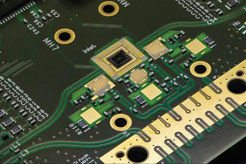
Intel’s latest announcement of the release of its Tunnel Falls quantum chip is a significant milestone in the development of silicon spin qubits. According to Intel, Tunnel Falls is the first publicly announced chip based on silicon spin qubits, which is a promising technology for the development of quantum computing. The chip is fabricated on 300mm wafers using Intel’s most advanced CMOS fabrication capabilities, including the use of extreme ultraviolet (EUV) lithography. The yield rate of the chip is also impressive, with a 95% yield rate across the wafer, in addition to voltage uniformity similar to a CMOS logic process. These developments demonstrate Intel’s commitment to advancing quantum computing technology and its ability to deliver on its promises.
The release of Tunnel Falls is a significant step forward in Intel’s strategy for developing silicon qubits. The chip’s fabrication on 300mm wafers using EUV lithography is a significant achievement, as it demonstrates the scalability of the technology. The high yield rate and voltage uniformity are also important factors in the development of a reliable and scalable quantum computing technology. The release of Tunnel Falls is likely to generate a lot of interest in the tech industry, as it demonstrates the potential of silicon spin qubits for quantum computing.
In conclusion, Intel’s announcement of the release of Tunnel Falls is a significant milestone in the development of silicon spin qubits for quantum computing. The chip’s fabrication on 300mm wafers using EUV lithography and its high yield rate and voltage uniformity demonstrate the scalability and reliability of the technology. Intel’s commitment to advancing quantum computing technology is evident in this latest development, and the release of Tunnel Falls is likely to generate a lot of interest in the tech industry.

 By
By
 By
By
 By
By
 By
By

 By
By
 By
By