
A bold wager on chip sovereignty for Tesla’s robotaxi and humanoid-robot roadmap
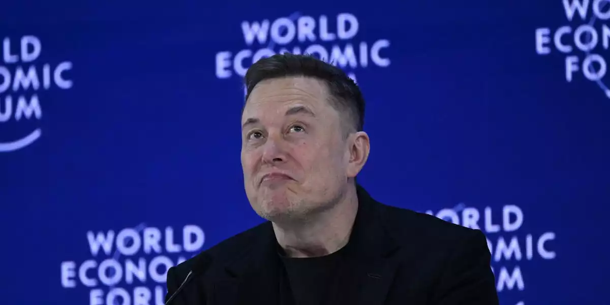
Elon Musk’s proposed “Terafab”—a fully integrated U.S. semiconductor foundry and advanced packaging complex—signals a decisive escalation in Tesla’s pursuit of end-to-end control over critical compute. The stated rationale is straightforward: Tesla expects demand for chips powering its next wave of products—robotaxi platforms and humanoid robots—to outstrip what even top-tier suppliers such as TSMC, Samsung, and Micron can reliably allocate.
If executed as described, Terafab would not merely be another capacity expansion. It would represent a strategic pivot toward becoming a rare modern hybrid: an automaker and AI company that also operates a high-volume semiconductor manufacturing and packaging ecosystem on U.S. soil. The reported initial target—100,000 wafers per month, with an aspirational path to 1 million wafers per month—places the concept in the realm of global-scale manufacturing rather than boutique internal supply.
The likely proximity to Tesla’s Austin footprint adds a practical dimension: co-location can compress logistics cycles, enable tighter hardware-software iteration, and reduce exposure to cross-border disruptions. Tesla’s recruitment for a semiconductor infrastructure manager underscores that this is moving beyond a thought experiment into early-stage execution planning.
Yet the ambition also raises a central question for investors, policymakers, and the broader technology supply chain: Can a company known for manufacturing reinvention translate that playbook into the unforgiving physics and economics of leading-edge semiconductors?
The engineering reality: fabs are not factories, and “integration” multiplies difficulty
Semiconductor fabrication is among the most complex industrial processes ever scaled. Tesla has proven adept at vertical integration in batteries, power electronics, and vehicle assembly—but chipmaking is a different category of challenge, defined by nanometer-scale tolerances, ultra-clean environments, and yield curves that can make or break economics.
Key operational hurdles implied by the Terafab concept include:
- Process complexity across multiple chip types: Building a facility that can produce logic, DRAM/memory, and specialized AI accelerators is materially harder than focusing on a single mature node or a narrow product class. Each additional process family introduces distinct tooling, chemistry, metrology, and yield-management requirements.
- Yield and ramp risk: The difference between a viable fab and a cash-consuming science project is yield stability. Even experienced foundries can take years to tune a new node or major process change; a greenfield entrant faces steep learning curves.
- Advanced packaging as a competitive necessity: Modern AI performance increasingly depends on packaging innovations (chiplets, high-bandwidth memory integration, advanced interconnects). Packaging can be a strategic advantage—but it is also another domain with specialized equipment, materials, and reliability constraints.
The most visible bottleneck is equipment. EUV lithography tools—dominated by ASML—carry multi-year backlogs, and allocation tends to favor established customers with proven ramp capability. Beyond EUV, a high-volume fab requires a dense ecosystem of deposition, etch, inspection, metrology, and test equipment, each with its own supply constraints and service needs. Materials supply adds another layer: high-purity silicon wafers, photoresists, specialty chemicals, and rare gases must be secured at scale with consistent quality.
Labor is the quieter constraint. The U.S. faces an acute shortage of experienced process engineers, tool owners, and maintenance technicians. Tesla may attempt to offset this with automation—potentially leveraging its robotics expertise for clean-room logistics and predictive maintenance—but fabs remain human-capital intensive, particularly during ramp and yield stabilization.
Capital intensity meets Tesla’s balance-sheet calculus—and the CHIPS Act opportunity
The projected $30 billion to $45 billion capital expenditure range places Terafab among the world’s most expensive greenfield industrial projects. That scale matters because Tesla is already funding multiple capital-hungry initiatives simultaneously: EV manufacturing expansion, robotaxi development, and Optimus-related R&D and production ambitions. With an estimated $20 billion cash burn this year cited by analysts, Terafab could force a financing conversation that Tesla has largely avoided since 2020.
The financial and strategic equation will likely hinge on three variables:
- Access to incentives and permitting speed: The U.S. CHIPS and Science Act provides substantial support for domestic semiconductor capacity. If Terafab aligns with federal and state priorities—jobs, onshoring, and supply-chain resilience—Tesla could pursue subsidies, tax credits, and accelerated approvals that materially change project economics.
- Phased build and node strategy: Investors will scrutinize whether Tesla targets leading-edge nodes immediately or adopts a staged approach, potentially starting with packaging and select mature-node components before moving up the complexity curve.
- Partnerships vs. pure independence: Despite the vertical-integration narrative, practical execution may require strategic alliances—with equipment vendors, materials suppliers, or smaller semiconductor players—to secure tool access, talent, and process know-how.
If Tesla succeeds, the competitive implications extend beyond its own products. Terafab could pressure the traditional foundry model by demonstrating that large OEMs—especially those building AI-centric systems—may seek sovereign, captive capacity for critical compute and memory. Even partial success could catalyze “friend-shoring” behavior across the U.S. industrial base.
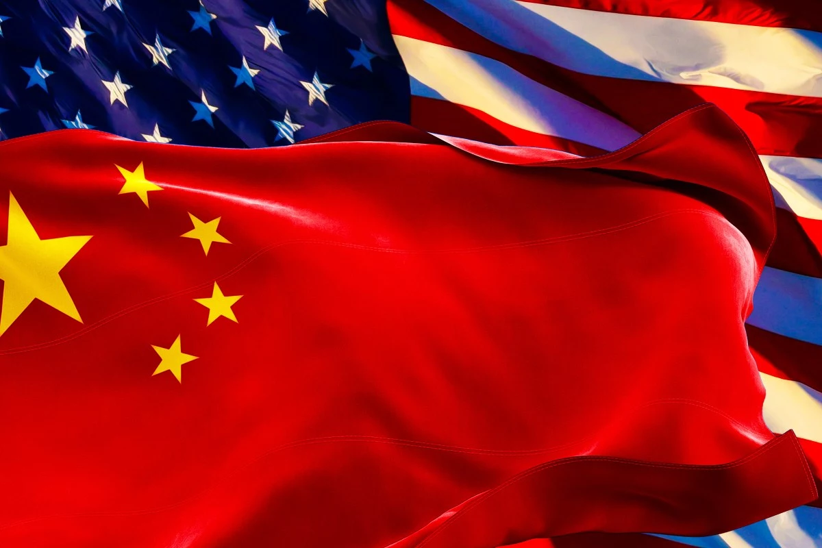
Geopolitics as the accelerant: Taiwan risk, export controls, and the new supply-chain playbook
The urgency embedded in a three-to-four-year timeline is difficult to separate from geopolitics. The semiconductor industry’s most consequential concentration risk remains the Taiwan Strait, where any disruption would reverberate through automotive, consumer electronics, cloud infrastructure, and defense supply chains. Terafab reads as a corporate hedge against a single-point-of-failure scenario—one that boards and governments increasingly treat as a planning assumption rather than a remote tail risk.
At the same time, the U.S. export-control environment is tightening, and technology decoupling pressures are reshaping procurement decisions. A domestic pipeline could insulate Tesla from sudden regulatory shifts affecting cross-border sourcing. However, “domestic” does not mean “self-sufficient”: critical tools and subcomponents still depend on a globally interlinked supply chain, including Dutch and Japanese dependencies in lithography and precision manufacturing.
Terafab, then, is best understood as a high-stakes attempt to redefine what resilience looks like for an AI-driven manufacturer: not just diversified suppliers, but controlled production of the compute stack itself. Whether Tesla can translate urgency into yields, and ambition into bankable execution, will influence how the next decade of U.S. semiconductor industrial policy—and private-sector supply-chain strategy—gets written.

 By
By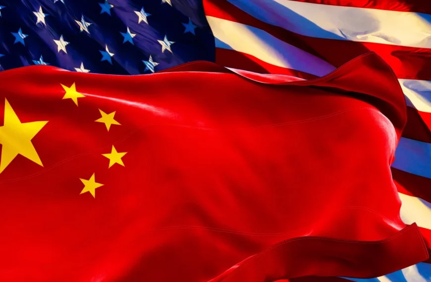
 By
By
 By
By
 By
By

 By
By
 By
By