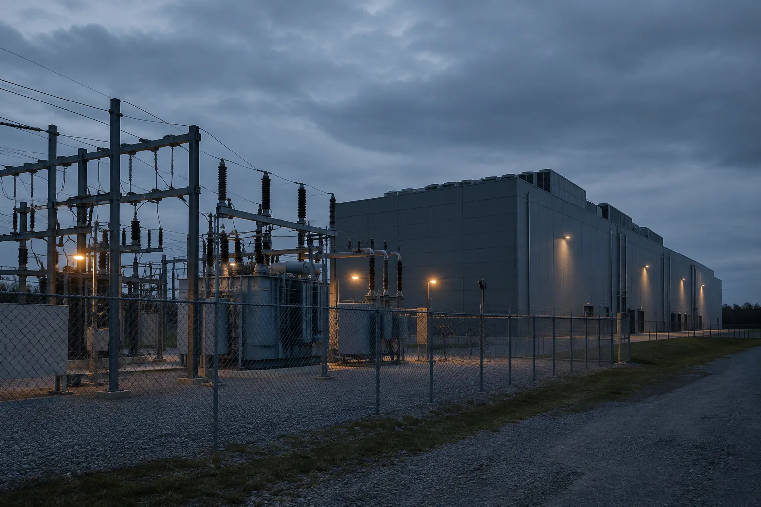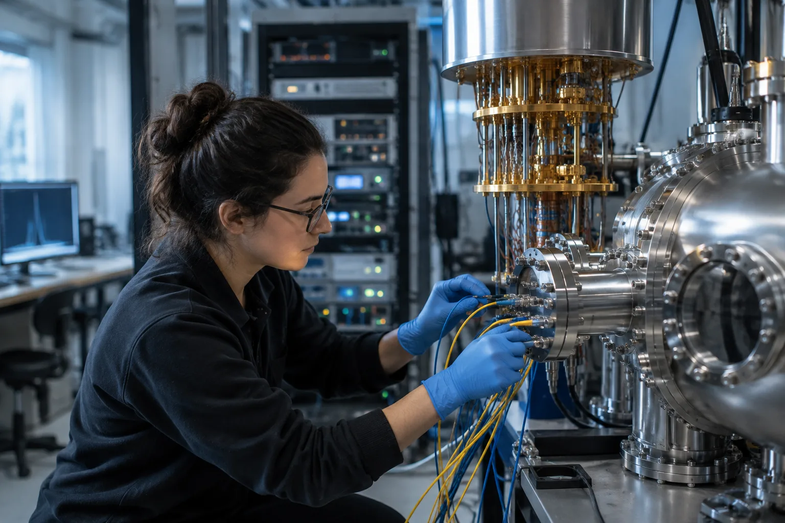



Applied Materials on Oct. 12 unveiled the Equipment and Process Innovation and Commercialization Center, or EPIC, at its Sunnyvale, California, campus: a roughly $5 billion semiconductor R&D project that brings together TSMC, Intel, Samsung Electronics, Micron, SK hynix, Broadcom, Advantest, SCREEN, KIOXIA, Besi and major universities in one shared development environment. The company says the 600,000-square-foot building includes nearly four acres of advanced cleanroom space and is designed to move new process technology more quickly from research into high-volume manufacturing.
That matters because EPIC is not a new chip or a new fab. It is a bet on a different way to solve one of the AI era’s hardest industrial problems: the gap between a promising breakthrough in materials or process technology and a manufacturable, high-yield production flow.
The real question for the industry is whether this model can materially compress that timeline, or whether EPIC becomes an expensive co-development hub whose payback depends on a small number of customers, projects and production wins.
Why the old development sequence is under pressure
AI demand is pushing semiconductor complexity up across logic, memory, interconnects, advanced packaging and power efficiency at the same time. A new model or accelerator can be announced years before the manufacturing process, yield, packaging and supply chain are ready for volume. At atomic-scale dimensions, materials and interfaces can behave differently than they did in earlier generations, which raises the cost of every mistake and makes slow handoffs more expensive.
Applied’s argument, laid out in its announcement and EPIC overview, is that chip development still separates foundational materials research, equipment and process development, and pilot manufacturing into stages that often learn sequentially. EPIC is meant to run more of that work in parallel, with materials researchers, equipment engineers, chipmakers, systems companies and university teams working inside the same secure environment.
If that works as intended, the gain is not just speed in the abstract. It means finding incompatibilities earlier, changing equipment while process choices are still open, and avoiding months or quarters spent optimizing a path that was never likely to scale. In the AI market, earlier learning can be almost as valuable as a headline performance leap.
What partners gain — and what Applied gains
The partner roster is a sign that the idea has industry weight. Applied lists TSMC, Intel, Samsung Electronics, Micron and SK hynix as founding partners. Innovation partners include Broadcom, Advantest, SCREEN, KIOXIA and Besi. Research partners include Arizona State University, Rensselaer Polytechnic Institute, Stanford, UC Berkeley and UCLA Samueli School of Engineering.
That network also formed over time, not in a single launch announcement. Applied had already announced Samsung as an EPIC partner in February 2026, TSMC collaboration in May, KIOXIA participation in September and the UCLA research partnership on Oct. 8. The Oct. 12 unveiling pulled those threads into one physical site and one operating model.
The commercial logic is two-sided. Chipmakers and systems companies get earlier access to materials and equipment learning that could reduce development risk. Applied gets earlier visibility into future process problems, which gives it a chance to shape tools and services around those needs before customers are locked into production schedules.
That is where the story gets more interesting than a building opening. EPIC may reduce duplicated experiments across the industry, but it also deepens Applied’s position as the equipment supplier hosting the shared environment. In effect, the company is offering a faster feedback loop while placing itself closer to the earliest process decisions.
Collaboration is the pitch; control is the tension
The unresolved issue is not whether major companies are willing to show up. It is how much they are willing to expose inside a facility that includes direct rivals and adjacent competitors.
TSMC, Intel and Samsung compete in advanced manufacturing. Micron and SK hynix compete in memory. Broadcom represents the systems side. Equipment and test partners have their own commercial interests. Universities want research translated into manufacturable processes. Those incentives align around solving harder physics and faster qualification, but they do not erase concerns about intellectual-property boundaries, data access, partner priority and roadmap separation.
The announcement does not spell out who owns resulting IP, how experiments are partitioned among competing chipmakers, what information is visible across the ecosystem or what access terms might apply to non-partner companies. Those are not side questions. They will shape who captures the value if the model works.
A smaller chip designer, for example, may benefit indirectly if tools mature faster and production ramps more smoothly. But it may not get the same early learning advantages as a top-tier foundry or memory partner. That matters for competition, because a shared R&D layer can reduce industry friction while still concentrating the best visibility among the biggest participants.
The scorecard that will matter a year from now
It is easy to overread the scale of the facility. Applied describes EPIC as the world’s largest facility dedicated to collaborative semiconductor process technology and manufacturing-equipment R&D, and the physical footprint is substantial: about 600,000 square feet, nearly four acres of cleanroom space and more than six million construction hours. But those are inputs to a development model, not proof that the model delivers faster chips, lower wafer costs or better yields.
The useful scorecard is operational. Has the time from concept to process qualification narrowed? How many pilot programs move into volume manufacturing? Do defect density and yield improve? Does wafer cost come down, or power efficiency improve, in ways that matter to customers? Can equipment-development cycles be shortened? Does the work produce repeatable revenue programs rather than one-off engineering exercises?
So far, those numbers are not public. Applied has not published a baseline for current time from materials breakthrough to qualification or high-volume manufacturing. It has not detailed the number and size of initial programs, the center’s operating cost or the expected return on investment. The roughly $5 billion figure is best read as a planned capital investment expected to scale as customer projects commence, not as a one-day outlay or guaranteed payback.
Independent coverage from the New York Post points to the strategic problem EPIC is trying to address, citing CEO Gary Dickerson’s view that AI-chip development can take more than a decade from breakthrough to production. What the unveiling does not show is whether EPIC will cut that timeline in practice.
For investors, chip designers and businesses waiting on future AI compute, networking or storage capacity, that distinction is the whole story. EPIC is a serious industry experiment in replacing serial semiconductor handoffs with a shared, secure learning loop. If it works, the benefits may appear indirectly through earlier equipment readiness, faster qualification and a less fragile supply chain. If it does not, the center will still stand as a very large reminder that coordination alone is not the same thing as commercialization.

 By
By
 By
By
 By
By
 By
By
 By
By

 By
By